A few minutes in air can start a clock on a delicate crystal. In some materials, oxygen and moisture begin changing the surface before researchers can finish turning a flake into a device. Protecting it is only half the problem: the cover must also let scientists see the crystal’s behavior and make electrical contacts without damaging what lies underneath.
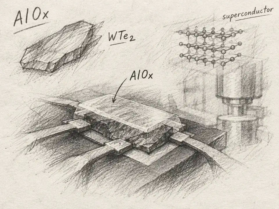
A new study explores an unexpectedly practical candidate for that double duty: aluminum oxide, deposited as a thin film by electron-beam evaporation. The researchers’ key move is to treat the coating not just as a lid, but as part of the fabrication process. It can shield a fragile material during processing, then be removed only where a contact needs to reach the surface.
The challenge is especially clear in rare-earth tritellurides, crystals whose exposed surfaces can oxidize rapidly. Unprotected LaTe₃ flakes thinner than 30 nm developed tellurium-oxide signals in measurements after less than a day in ordinary laboratory air. The capped flakes, by contrast, showed nearly unchanged Raman spectra over 6 to 10 days. Raman spectroscopy works here like a material fingerprint: changes in the light scattered by a sample can reveal that its chemical or structural character is shifting.
For the more air-sensitive ErTe₃, the difference was sharper. Unprotected flakes developed oxidation-related signals and lost spectral contrast within about an hour. Capped samples showed no measurable degradation over several days under the same conditions. Under a microscope, the unprotected LaTe₃ also developed bubbles and delaminating layers—damage absent from the protected samples.
But a cover that works on one flake can still fail at its edges. Oxygen can slip beneath a coating where it does not seal against the crystal and then spread between the layers. The team found that a 130 nm AlOx cap did not reliably protect thicker LaTe₃ flakes on silicon dioxide: oxidation-related signals appeared after 41 to 86 hours. Switching the substrate to crystalline sapphire changed the result. A 90 nm flake showed no evidence of oxidation after 120 hours in air. Across 26 flakes, 32 of 37 measurement points remained largely unchanged. Cracks, scratches, and overlapping flakes accounted for some exceptions.
That substrate dependence is a reminder that “put on a protective layer” is not a complete recipe. How the coating forms—and whether it closes the vulnerable edges—matters. The researchers suspect AlOx forms a more effective interface on crystalline sapphire than on amorphous silicon dioxide, where gaps may let oxygen or water through. The coating is promising, but not a universal seal that can be assumed to work identically on every surface.
The team then tested a thinner cap against a different demand: preserving access to a material’s optical response. WTe₂ can support plasmonic behavior—collective motions of its electrons that interact with light. A thick cover could interfere with measurements made close to the surface. The researchers applied just 3 nm of AlOx and used near-field optical microscopy to examine the capped crystal. Its thickness-dependent optical contrast remained visible, and Raman measurements showed no measurable shifts or broadening beyond experimental uncertainty.
The most consequential twist came in device fabrication. Standard patterning can expose sensitive crystals to photoresist, solvents, and other processing steps. Here, the thin AlOx layer first acts as a protective mask. During development of the patterned resist, the developer removes exposed AlOx in the regions intended for contacts, while the rest of the crystal remains covered. The process could let a lab make top contacts without first stripping protection from the entire surface.
To test that idea, the researchers fabricated devices from an iron-based superconductor, FeTe₀.₅₅Se₀.₄₅. Devices made through a 3 nm protective layer retained a superconducting transition near 14 K, comparable to conventionally processed samples. The transition width was 0.47 K for the device made through the sacrificial layer, versus 0.77 K for the post-fabrication-encapsulated comparison. In this test, the protected route did not just preserve superconductivity; the narrower transition suggested improved device quality.
What might this unlock? If a fragile crystal can stay protected from exfoliation through contact-making and measurement, researchers may be able to investigate materials that are difficult to handle with transfer-based covers. The approach uses a familiar deposition technique and fits conventional lithography, rather than requiring precise stacking and alignment of a separate protective crystal. It might make experiments easier to reproduce and could support larger-area fabrication. Those are possibilities, not demonstrated production outcomes: the study establishes a method across several material systems, not a manufacturing line for finished devices.
The price of the simpler process is careful matching between coating, material, and substrate. The paper notes that high-quality electrical contacts across a broader range of quasi-two-dimensional materials still need to be established. Preliminary work on monolayer flakes also needs optimization; the researchers found no clear evidence that the coating fully prevented oxidation in the thinnest WTe₂ region. A cap that succeeds on a thicker flake may not protect a single atomic layer well enough.
So the frontier is not simply making a better shield. It is designing a shield that can disappear exactly where a device needs contact, without letting the outside world reach the rest of the material. A few nanometers of oxide may help delicate crystals survive the journey from discovery to experiment. Whether that small layer becomes a broadly useful building block will depend on sealing the edges, refining the process for the thinnest flakes, and proving it across many more materials.