An old optical disc has a deceptively simple promise: put information in a small, stable object, then leave it alone until someone needs it. The hard part is fitting more data into each speck without making it too difficult to write or read. A new experiment takes an unusual route around that problem. Instead of using a laser to burn each data point in turn, researchers pattern a crystal with a fabrication process more familiar from making tiny electronic devices—and let the resulting fluorescent ions carry the bits.
The storage material is a crystal of yttrium aluminum garnet, or YAG. To write a pattern, the team used electron-beam lithography to carve openings in a thin resist mask. They then implanted ions through those openings into the crystal. After heating the material to activate the fluorescent centers, the patterned regions could be read by shining light on them and detecting the glow. The key move is to separate the making of each tiny data location from the optical process used to read it.
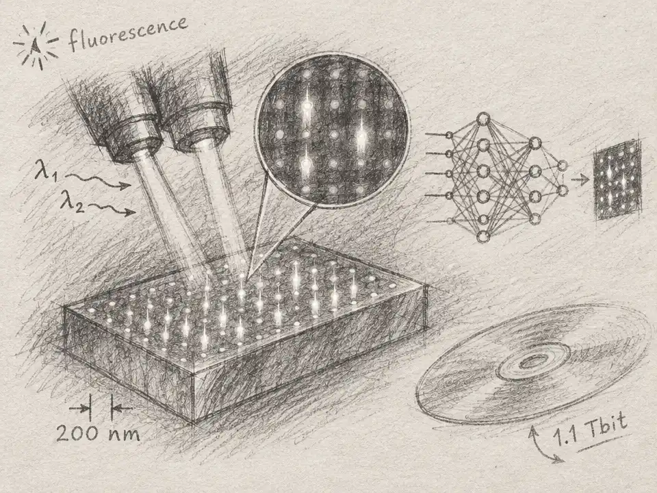
That separation opens up two ways to put more information in the same area. First, a site can glow at one of four brightness levels, rather than simply being on or off. The size of each mask opening helps control how many fluorescent ions land in a location, changing its brightness. Four distinguishable levels can represent two bits per site. In one demonstration, the team used openings with side lengths of 80, 110, and 140 nm to encode the three nonzero levels; an unimplanted site represented zero.
Second, the researchers wrote separate patterns using two kinds of rare-earth ions, cerium and praseodymium. Each responds to different combinations of light and fluorescence, allowing the researchers to select one data pattern or the other. Think of it as adding another track in the same patch of crystal: brightness provides several possible marks, while the ion’s optical signature identifies which channel is being read. In the demonstrated system, the two channels could be addressed independently by choosing the excitation light and the range of emitted light to detect.
Then comes the catch. The fabricated sites can be closer together than an ordinary optical microscope can cleanly distinguish. In the densest pattern, sites were spaced 200 nm apart, and their fluorescent signals blurred into one another. The image no longer looked like a tidy row of separate dots. Instead of trying to sharpen every dot optically, the team trained a neural network to interpret the pattern around each location. Its input included a 3-by-3 neighborhood, so it could use nearby signals to infer the brightness level at the center.
That computational reading recovered information hidden in the blur: validation accuracy reached 96.57% for four-level decoding and 97.58% for binary decoding. With 200 nm spacing, four brightness levels, and two wavelength channels, the researchers calculated an areal density of 10 Gbit/cm2. Scaled to the footprint of a standard 120-mm optical disc, that density corresponds to approximately 1.1 Tbit—about five times the capacity of a conventional single-layer Blu-ray disc.
The scale matters as much as the headline number. The team patterned arrays measuring 3.5 × 3.5 mm2, not a complete disc. The 1.1 Tbit figure is a capacity estimate based on applying the measured density across a disc-sized area. It is not a demonstration of a consumer-ready disc holding that much data. The researchers also report high-fidelity readings at wider spacing: with four brightness levels and 500 nm spacing, decoding fidelity was 94.26% for the praseodymium sample and 97.69% for the cerium sample. At the tighter 200 nm spacing, machine learning helps unlock higher density, but does not eliminate the challenge of reading every bit correctly.
And the write process is not yet a quick desktop operation. Each new ion channel requires another patterned mask and implantation step. After implantation, the crystal was heated in air to 1200 °C and held there for 8 h to activate the fluorescent centers. Electron-beam lithography offers precise patterning, but the authors identify large-area fabrication and parallel optical readout as steps still needed to reach wafer-scale memory. The experiment shows a path to putting dense patterns over millimeter-scale areas; it does not establish how fast, cheaply, or uniformly such patterns could be produced at commercial scale.
There is also a difference between making a bright pattern and proving a dependable archive. The researchers demonstrate how to encode and decode information, but do not report a long-term aging test of the stored data or the energy use of a complete storage system. A solid optical medium that does not need continuous power while sitting on a shelf could be attractive for “cold” data—information rarely accessed but worth keeping. Whether this particular design can deliver that benefit over years or decades remains an open question.
The decoder raises a subtler issue. At high density, a site’s meaning depends partly on its neighbors, and the network learns to interpret those surrounding patterns. That may be a powerful way to recover data from crowded signals. But a working archive would need reliable decoding across different patterns and devices, not just successful validation in the reported experiment. The current accuracy figures make the promise visible while marking the distance still to travel.
For now, the most interesting idea is not simply that a disc might hold more. It is that storage can be designed as a conversation between fabrication and inference: lithography places fluorescent marks more tightly than ordinary optics can resolve, and a learned decoder reconstructs their message from the glow. The possible prize is dense, low-maintenance archival storage. The price is a demanding manufacturing chain—and a reader that must prove it can distinguish the message, consistently, after the crystal has left the lab.