Imagine asking a piece of glass to change its mind about where light should go. In a lab, researchers projected a new pattern of light onto a programmable waveguide—and taught the same chip to route optical signals in several different ways. The striking part is not just that the chip can be reconfigured. It is that its designers used measurements from the real device to help work out each new design, rather than trusting a computer simulation to get every detail right.
That matters because photonic chips—devices that process or guide information using light—are often made for a particular job. To give one a new layout, engineers may need to design, fabricate, and test another device. The process can be slow, and a design that works beautifully in simulation may behave differently once etched materials and tiny imperfections enter the picture. The new approach offers another possibility: build a waveguide that can be reshaped after fabrication, then train it to do a new task when needed.
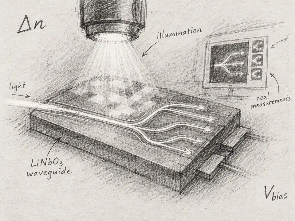
The experimental device begins as a thin, flat slab of lithium niobate, a material whose optical properties respond to electric fields. Unlike a conventional chip with fixed etched pathways for each function, this slab’s refractive index—the measure of how it bends light—can be adjusted across roughly 104 effective regions. Researchers project a spatial pattern of illumination onto a light-sensitive layer above the slab. Where the layer is illuminated, its electrical conductivity changes. Under an applied voltage, that redistributes the electric field through the stack, changing the lithium niobate’s refractive index in the corresponding regions.
The result is a kind of adjustable landscape for light. A programmed patch can nudge a beam, divide it among routes, or help separate different optical patterns. To change the landscape, the team changes the projected illumination pattern. The device’s refractive-index pattern can be reset in about 1.5 s, then set to a new one. No new chip has to be fabricated for each demonstrated function—though the programmable chip itself still requires careful fabrication.
Working out the right pattern is an optimization problem: specify what the light should do, try a pattern, measure the output, and adjust. The researchers combined a digital model with measurements from the physical waveguide. The model helped calculate how to update the pattern; the real device supplied feedback about what actually happened. That loop is important because it can compensate for discrepancies between simulation and hardware, including imperfections in fabrication or calibration.
After an initial dataset was collected, the optimization converged in around 100 iterations, taking about 10 to 20 minutes for the reported tasks. In one example, training a four-input, four-output spatial-mode permutation took around seven minutes. The team demonstrated several functions on the same device: rearranging four or eight optical modes, separating four Hermite–Gaussian modes, and performing 4 × 4 matrix–vector operations in the optical-power domain. A mode is a particular spatial pattern of light; sorting modes is a way to route signals that share a channel but differ in shape.
The researchers also changed how the device handled wavelength. It could perform the same transformations across the 1500–1600 nm window, and it could direct 1310 nm and 1550 nm light into different outputs, with maximum crosstalk of −8.4 dB. Crosstalk is unwanted leakage: light intended for one output showing up in another. For the four-mode spatial permutation, crosstalk reached −27 dB; for the eight-mode permutation and four-mode separation, it was −13 dB. These results suggest that one reconfigurable platform could, in principle, take on jobs that otherwise call for multiple specialized optical components.
But the demonstration is a laboratory prototype, not a ready-made communications chip. Its programmable index contrast was about 1.7 × 10⁻³, which limits how compactly it can manipulate light and how many modes it can handle. The projected illumination pixels had a pitch of 9 µm, and electric fields spread sideways through the layers, blurring the programmed pattern. Measurements also came with an important caveat: the team recorded output intensity, not the full optical phase, and assumed a flat output phase when estimating performance. Its insertion-loss estimates should therefore be treated as lower bounds, not definitive measurements of the power lost.
There is an energy and speed price, too. The current pattern must be held in place with both illumination and electrical bias; the reported static power use was approximately 3 mW of optical power and approximately 2 mW of electrical power. Switching patterns took about 1.5 s. The team projects that design improvements could raise the index change to 10−2 and make 128 × 128 mode transformations possible in simulations on a 5 cm × 5 cm footprint. Faster switching, potentially reaching the kilohertz level, is also a projection—not a demonstrated result. The paper notes that optical circuit switching in data centers would require switching times on the order of 10 µs to rival electronic packet routing, a tougher target.
That gap is the frontier: not simply making a chip that can change its optical behavior, but making it fast, efficient, precise, and scalable enough to be useful outside the lab. A more conductive light-sensitive layer could speed up switching, but the authors warn that it could also raise electrical power use. The device can also retain a weak, reversible trace of a pattern after prolonged exposure; uniform illumination erases it, but memory like this matters when precise reprogramming is the point.
Still, the experiment hints at a different way to build optical hardware. Instead of carving every desired behavior permanently into a separate chip, engineers might fabricate a versatile optical surface and tune it for the task at hand—using the device’s own measured behavior to guide the tuning. That could make adaptable photonic functions practical where manufacturing a custom component for every job is not. For now, the chip has shown that light can be given new routes after fabrication. The next test is whether those routes can become fast and economical enough to matter in the systems that need them.